

Abstract
A new industrial series transfer mold type mini DIPIPMTM developed for applications like general inverter and servo for small capacity industrial motor drive or package air conditioner is presented in this paper. The new DIPIPMTM is designed to compatible with current mini DIPIPMTM Ver.3 and Ver.4 package outline, and taken external BSD(Bootstrap Diode) chips and temperature measurement function(eg. thermistor) inside to help realize cost down for inverter drive system by reducing peripheral electronic parts and PCB board size. By applying the VLD(Variation of Lateral Doping) structured 6.1th generation IGBT chip technology, both power loss and chip size are reduced compared with conventional mini DIPIPMTM products. And product line-up has extended to 50A current rating with the same package size (Fig.1), which used to be 30A in present line-up.
1. Introduction
Since its first introduction in 1997, DIPIPMTM developed by Mitsubishi Electric has been used in a variety of inverter drive applications, from white goods such as air-conditioner, washing machine etc. to industrial motors.
In recent years, inverters for motor drive system aiming at energy saving and high performance are progressing broadly. Mitsubishi Electric Corporation released the mini DIPIPMTM Ver.3 and Ver.4 series products for industrial motor and package air conditioner in 2000, and made a huge contribution for the miniaturization of inverter control system. Like what has always been considered in inverter system designed for consumer applications, cost-performance ratio are more and more emphasized in small capacity industrial applications as well. Integration of multiple functionally related electronic parts together while without sacrificing of reliability and system space is one of the most effective ways to realize cost reduction.
Based on this concept, Mitsubishi Electric Cooperation developed a new industrial series transfer mold type mini DIPIPMTM PSSxxS71F6 & PSSxxS51F6 that was designed to have BSD(Bootstrap Diode) chips and temperature measurement function(eg. thermistor) embedded while still compatible with current mini DIPIPMTM Ver.3 and Ver.4 products in package configuration.
The outline view of Industrial serises 600V mini DIPIPM is shown in Fig.1 and Fig.2.
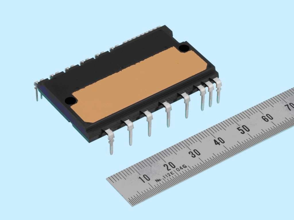
Fig.1 Outline view of PSSxxS71F6
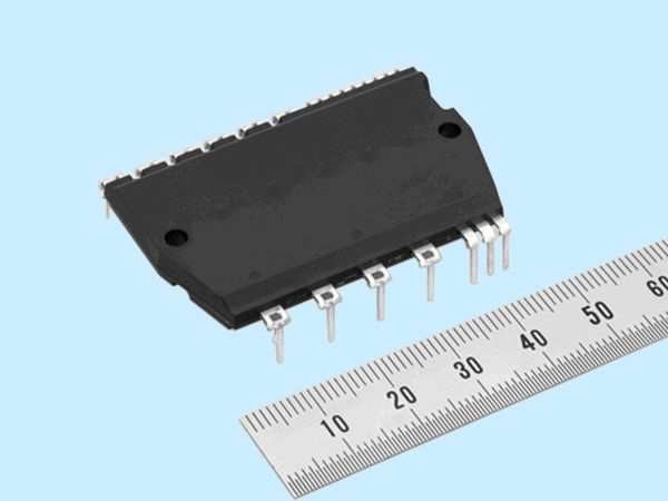
Fig.2 Outline view of PSSxxS51F6
2. Technology adopted in New Industrial series MINI DIPIPMTM
2.1 Power chip
New industrial series mini DIPIPMTM adopts the 6.1th generation Carrier Stored Trench-Gate Bipolar Transistor (CSTBTTM) chip technology that constructed on the basis of its predecessor: the 6th generation chip and incorporated a highlighted narrow terminal structure, in order to get the equivalent current carrying ability in a smaller chip. This new structure achieves a terminal size reduction of about 50% compared with conventional CSTBTTM (Field Limited Ring terminal structure).
Fig.3 shows the basic cross section structure of the CSTBTTM chip used in the new industrial series mini DIPIPM™.
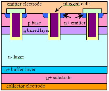
Fig.3 Structure of CSTBTTM chip
The IGBT chip used in the new industrial series mini DIPIPMTM was designed to have a plugged cell merged structure, in order to reduce the input gate capacitance and ensure a higher short circuit (SC) withstand capability to better fit the needs of industrial application.
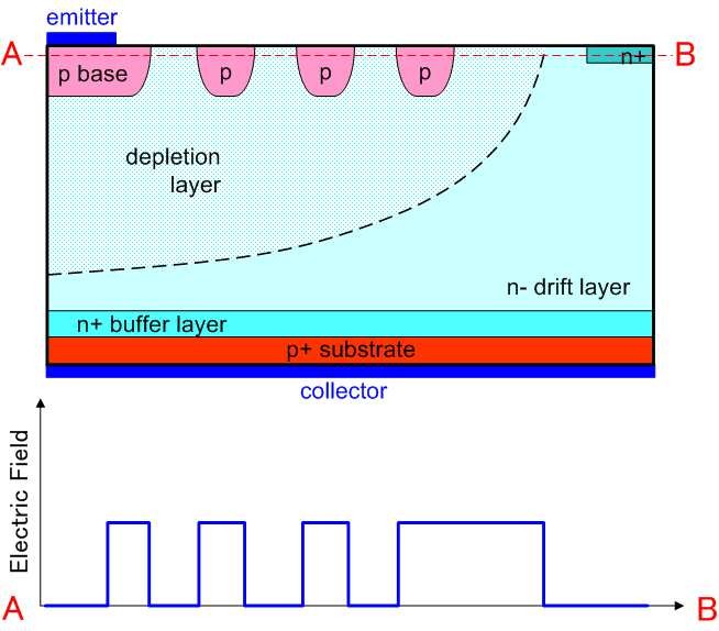
Fig.4 Field Limited Ring terminal structure Fig.5
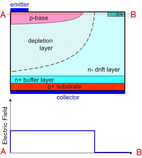
Fig.5 Variation of Lateral Doping structure
The Field Limited Ring (FLR) terminal structure is usually used in the traditional CSTBTTM, as is shown in Fig.4.
When the positive bias voltage is applied to the collector electrode on the basis of the emitter electrode, depletion layer is extended from the p-base region to the outer p-region.
Correspond to the increase of positive bias voltage, depletion layer is reached to the neighboring p-region. Consequently the breakdown voltage is proportional to the number of FLR. As is shown in Figure 4, the specific area of the p-region is not depleted. Thus the area is not contributed to the increase of the sustaining voltage.
In order to make full use of this p-region, that can realize chip size shrinking, a new Variation of Lateral Doping (VLD) terminal structure is developed to replace the conventional FLR. The VLD structure is shown in Fig. 5.
This new structure is really formed in P base layer which has a concentration gradient from the emitter electrode side. When positive voltage is applied to the collector electrode on the basis of an emitter electrode, the depletion layer has the feature which extends in the whole p- base region. Thus the electric field distribution of the VLD structure shows a rectangle shape. Moreover, the VLD structure does not contain an invalid region that functionally blocking voltage, as a result, short length of the VLD is able to withstand high collector voltage. This means that the terminal length of the VLD can be designed as short as half that of the FLR for same blocking voltage.
Due to the application of this technology, IGBT chip size was reduced about 20% compared with current mini DIPIPMTM products. The power loss of a single IGBT chip was reduced about 10% compared with current 30A product and current ratting line-up was successfully extended to a maximum of 50A with the same package body, which used to be capable to reach only 30A. Fig.6 shows the power loss comparison.
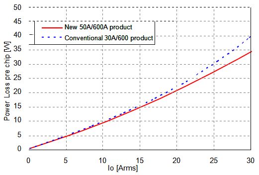
Fig.6 New DIPIPM(50A/600V) IGBT power loss Vcc=600V,VD=VDB=15V,fc=10kHz,P.F=0.8,MR=1,
Tc=100deg,3-phase PWM modulation
2.2 Embedded Bootstrap Diodes (BSD)
Incorporate BSD chip into a DIPIPM that designs for industrial applications will face challenges from mainly two aspects.
a) The output voltage generated through BSD chip must stable enough to ensure reliable operation of high-side IGBT gate drive IC, even in the toughest situation that inverter driver could experience in industrial field application, like occasional motor lock etc.
As a counter measure for this challenge, our BSD chip is designed with an integrated 20Ω current limiting resistor, lower resistance to ensure a more stable high-side power supply.
Fig.7 shows the IF-VF curve of BSD.
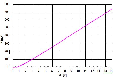
Fig.7 IF-VF curve for bootstrap diode 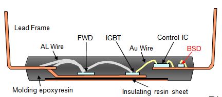
Fig.8 Structure of new industrial series mini DIPIPMTM
b) There must have enough space available near high-side driver IC to accommodate BSD chip.
This challenge is solved by the evolution of our IC process technology. To achieve control IC chip size shrinking, the new generation 0.5µm process HVIC (current process: 1.3µm) which has some world leading technologies like divided RESURF structure is used. As a result, the
chip size of new control IC was reduced about 30% compared to the current products. Fig.8 shows the internal structure of new industrial series mini DIPIPMTM.
2.3 VOT function(Analog output voltage of temperature)
Another conception devoted to the design of new industrial series mini DIPIPMTM, for the purpose of system cost reduction is the integration of temperature measurement function. With the use of laser-trimming technology, the high precision temperature converting circuit is built into the low-side control IC (LVIC) that enables it to provide an analog voltage output (VOT) signal by sampling the temperature of LVIC chip. This makes it possible to eliminate the traditional external thermal resistor that helps to reduce the system cost.
The accuracy of temperature output signal can reach ±5%, and by following that analog output voltage signal, it is possible to use the DIPIPM at a junction temperature much closer to the tolerable maximum rating value than conventional products and makes it easier for heat dissipation design.
Fig.9 shows the output characteristic of VOT.
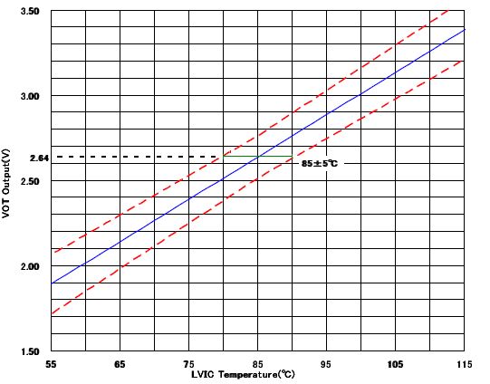
Fig.9 VOT characteristic of new industrial series mini DIPIPMTM
3.Electrical circuit configuration and components
The internal circuit of new industrial series mini DIPIPMTM is composed of IGBTs and FWDs (Free Wheel Diode) in a three-phase inverter structure together with new generation control ICs and three BSDs.
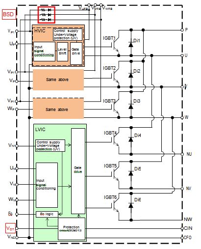
Fig.10 Internal block diagram of new industrial series mini DIPIPMTM
Control ICs are incorporated with basic functions such as IGBT drive, control power supply under-voltage (UV) lockout etc. Optimized designs, like logic filtering function and high precision short circuit (SC) protection are also used to achieve enhanced input noise immunity and expanded current working range.
High-side driver uses embedded HVIC where high-low voltage level shift circuits are integrated that enables direct drive of IGBT without opt-coupler parts. In addition, the soft switching effect has been obtained by optimizing the drive capability, which helps to suppress the switching noise.
Fig.10 shows internal block diagram of new industrial series mini DIPIPMTM.
4. Electrical characteristics
The main electrical characteristics (inverter part and control part) of new industrial series mini DIPIPMTM (50A/600V) are indicated in Table 1.
5. Conclusions
To fit the needs of industrial inverter applications, we designed a new series BSD and temperature measurement function (VOT) embedded mini DIPIPMTM. By adopting the 6.1th generation CSTBTTM chip that characterized by the Variation of Lateral Doping (VLD) terminal structure, we successfully achieved 20% chip size shrinking and 10% power loss reduction and have a package finish the same as conventional mini DIPIPMTM.
This development is sure to make further contribution to the design of low cost, high
reliability and miniaturization of inverter system used in industrial applications. We will continuously make efforts to develop more excellent devices to realize power loss reduction and save natural resources in many fields.
6. Literature
[1]G. Majumdar, et al.,"A New Generation High Performance intelligent Power Module", 1992 PCIM Europe.
[2]S. Shirakawa, T. Iwagami, H.Kawafuji, M. Seo, K. Satoh ''A New Version Transfer Mold- Type IPMs with Compact Package'' 2005 PCIM China.
[3]Toru Iwagami, Katsumi Satoh, Kou shomei, Hisashi Kawafuji, Shinya Shirakawa, Tomofumi Tanaka '' A Development of 30A/600V Super mini DIPIPMTM '' 2006 ipemc,
[4]T.Takahashi, Y.Yoshiura '' The 6th-Ganeration IGBT&Thin Wafer Diode for New Power
Modules” 2011 Mitsubishi Electric ADVANCE June 2011,
[5]T.Tanaka, T.Shiraishi, '' Development of 1200V large DIPIPMTM Ver.4” 2011 Mitsubishi Electric ADVANCE June 2011
Table1. Main electrical characteristics (Tj=25C, unless otherwise noted) of PSS50S71F6 (50A/600V)
Inverter Part:
|
Item |
Symbol |
Condition |
Min. |
Typ. |
Max. |
Unit |
|
|
Collector-emitter saturation voltage |
VCE(sat) |
VD=VDB15V VIN=5V, IC=50A, |
Tj=25°C |
- |
1.50 |
2.00 |
V |
|
Tj=125°C |
- |
1.60 |
2.10 |
||||
|
FWD forward voltage |
VEC |
VIN=0V, -IC=50A, Tj=25°C |
- |
1.60 |
2.10 |
V |
|
|
Switching time |
ton |
VCC=300V, VD=VDB=15V IC=50A, VIN=0↔5V Tj= °C Inductive load (upper-lower arm) |
1.05 |
1.65 |
2.30 |
µs |
|
|
trr |
- |
0.60 |
- |
||||
|
tc(on)125 |
- |
0.50 |
0.80 |
||||
|
toff |
- |
2.00 |
2.60 |
||||
|
tc(off) |
- |
0.40 |
0.90 |
||||
Control (Protection) Part:
|
Item |
Symbol |
Condition |
Min. |
Typ. |
Max. |
Unit |
|
|
Circuit current |
ID |
VD=15V, VIN=5V VD=15V, VIN=0V |
VN1-VNC |
- |
- |
6.00 |
mA |
|
VN1-VNC |
- |
- |
6.00 |
||||
|
IDB |
VDB=15V, VIN=5V VDB=15V, VIN=0V |
V*FB-U/V/W V*FB-U/V/W |
- |
- |
0.55 |
||
|
- |
- |
0.55 |
|||||
|
Control supply under -voltage protection (P-side/N-side) |
UVDt |
Tj£125°C |
Trip level |
10.3 |
- |
12.5 |
V |
|
UVDr |
Reset level |
10.8 |
- |
13.0 |
|||
|
ON threshold voltage |
Vth(on) |
Applied between UP,VP, WP-VNC UN,VN,WN -VNC |
- |
2.1 |
2.6 |
V |
|
|
OFF threshold voltage |
Vth(off) |
0.8 |
1.3 |
- |
V |
||