
Abstract
In this paper, we introduce the technology applied to the 7th generation IGBT modules with miniaturized size and reduced weight. For the chip, latest 7th generation IGBT and 7th diode are applied, where both static and dynamic losses are reduced. For the packages, a novel insulation and heat radiating structure are employed to achieve a high density chip mounting. As a result, 7th generation IGBT module makes it possible to double the current rating with the same package size. The weight is reduced by 45% from conventional module.
1. Introduction
In power electronics, IGBT modules are used for various purposes and in various places. This trend will continue for a while. For this tendency two basic requirements arise for IGBT modules as a market demand. The first request is a “miniaturizing” in order to ease the design of user’s system geometrically. The Second request is a “weight saving” for increasing the possibility of IGBT modules in applications where equipment weight has a restriction. In order to meet these requirements, the next generation industrial IGBT modules, called the 7th generation, was developed. The concept is to support various applications. The chips used in the modules are the 7th generation IGBT and Relaxed Field of Cathode (RFC)- planar anode diode [1-2]. In order to improve the performance, these chips are thinner than previous versions. In the module’s package, a novel insulated thermal radiation material is employed as base plate structure of the package. These techniques are allowing miniaturization and weight saving of 7th generation IGBT modules as reported below.
2. Chip technologies
2.1. 7th generation IGBT
The 7th generation IGBT chip is applied to the optimized Carrier Stored Trench-Gate Bipolar Transistor (CSTBTTM) [3] technologies. The thickness of the chip is thinner than the previous version with Light Punch Through (LPT) structure on advanced thin wafer technology [4-5]. The 7th generation IGBT chip has mainly two improvements from 6th generation IGBT chip as follows.
First, the 7th generation IGBT chip has a reduced thickness. By reducing the thickness of IGBT chip a reduction of static and dynamic losses of IGBT chip can be realized. However chip thickness and short circuit capability are lined by a trade-off. In order to reduce the thickness of the IGBT chip with required short circuit capability, short circuit energy must be decreased. The short circuit energy is a multiplication of voltage, current and time during short circuit operation. Since the voltage and time are fixed by the application, the maximum short-circuit current should be reduced in order to keep short circuit capability. In the 7th generation, by improving process, the maximum short-circuit current was reduced without reducing the minimum of saturation current (IC(SAT)). Thus, 7th generation IGBT chip has improved the trade-off relationship between the on-state saturation voltage (VCEsat) and the turn-off switching energy losses (Eoff) and turn-on switching energy losses (Eon) with sufficient
short circuit capability. Second, the unit cell design was optimized for the purpose of improving the trade-off relationship between Eon and maximum recovery dv/dt. Reducing the dv/dt has an effect on suppressing the EMI irradiation noise from equipment. If one needed to reduce the EMI irradiation noise, the dv/dt would be reduced by increasing the gate resistance (RG). Hence, reducing the dv/dt will invite large Eon with slow time. Then, in the 7th generation IGBT chip, optimization of the unit cell design can improve this trade-off, and Eon is lower than previous generation when these are evaluated on the same dv/dt condition.
As a result, in 7th generation IGBT chip, reduction of the static and dynamic losses without sacrificing the short-circuit capability was realized, together with the improvement of the trade-off relationship between Eon and the turn-on dv/dt.
2.2. 7th generation diode
To reduce the thickness of diode it is important to reduce the static and dynamic losses simultaneously like IGBT. However, carriers in n- layer disappear very rapidly during reverse recovery. This quick expansion of depletion layer is the root cause for snap-off and oscillation phenomena. Then, in 7th generation IGBT module, a RFC diode is applied.
Fig. 1 shows the cross sectional view of conventional diode and RFC diode. There are two big differences between these structures. First, RFC diode has unique structure in cathode side of the chip. P layers are inserted partially and alternately in former n+ layer. This shallow p and n+ alternating layer can relax the expansion of depletion layer in n- layer by holes injection from p layers. Then, RFC diode doesn’t have snap-off and oscillation waveforms even if conventional diode has these waveforms. Second, RFC diode is thinner than conventional diode by 20%. Thus, RFC diode has improved the trade-off relationship between the forward voltage (VF) and the reverse recovery energy losses (Err) and reverse recovery charge (Qrr). In 7th generation, the chip was shrunk for miniaturizing the package.
An experimental comparison waveform between conventional diode and RFC diode is shown in Fig. 2. No snap-off and oscillation phenomena can be seen in the RFC diode waveform. Then, reducing the level of the noise can be expected. Loss comparison is shown as trade- off curve between VF vs. Qrr in Fig. 3 and VF vs. Err in Fig. 4. These data show that the trade- off characteristics of RFC diode are better than conventional one. This improvement enables to optimize the diode chip, and then Qrr became smaller. Thus, it is also possible to reduce Eon, because of reduction of the part of Eon determined from Qrr. These data show that RFC diode can reduce the static and dynamic losses without snap-off and oscillation phenomena.
As a result, in 7th generation IGBT module, reduction of the static and dynamic losses without snap-off and oscillation phenomena was realized.
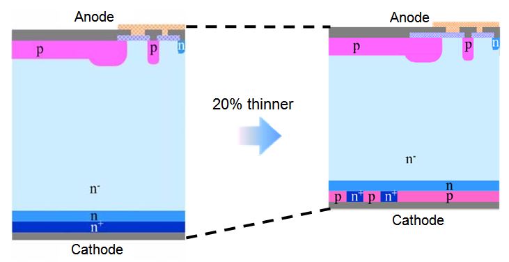
Fig. 1. Cross section view of conventional diode (left) and RFC diode (right).
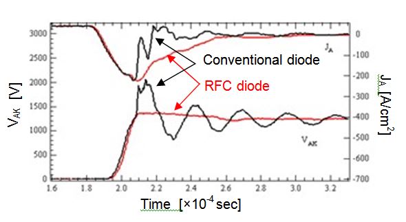
Fig. 2. Experimental recovery waveforms of 1700V diodes.
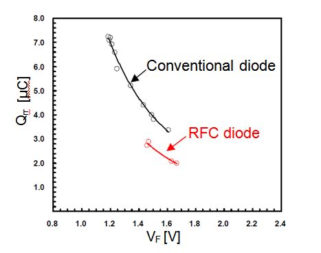
Fig. 3. Experimental results for trade-off characteristics between VF vs. Qrr of 1200V diodes.
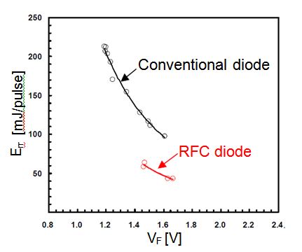
Fig. 4. Experimental results for trade-off characteristics between VF vs. Err of 1200V diodes.
3. Package technologies
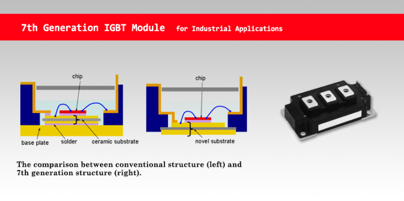
Heat transfer related technology, such as ceramic production and reduction of thermal contact resistance, is progressing. Along this trend, in 7th generation IGBT modules an optimized substrate and structure will be applied. Fig. 5 illustrates the comparison between conventional IGBT module structure and novel 7th generation module structure. There are mainly three differences between these two structures.
First, without using a Cu base plate, Cu foil thickness was increased for the based substrate instead. The elimination of Cu base plate enables weight saving. In 1200V 600A, the weight of previous package is 580g, and the weight of 7th generation package is 320g. Then, 45% decreasing in weight at same current rating. Second, the material of the substrate is changed to a higher toughness. This improvement allows the wider and thinner substrate area than before. Since this also means the removal of some internal bonding wire between each substrate, self-inductance was reduced. Third, the thickness of circuit pattern on the substrate is increased. Then, the width of this pattern required for current conduction can be reduced. This improvement also enables a miniaturized package. 7th generation IGBT module was realized by keeping the conventional external package outline. Thus, 62mm × 108mm package was used in 1200V 300A product in previous generation, but it is used in 1200V 600A product in 7th generation. In other words, 7th generation IGBT module makes it possible to double the current rating with the same package size. On the other hand, higher surge voltage problem occurred at conventional package if supplied larger current, by the increase of di/dt. As a countermeasure to this problem, a 33% reduction of the parasitic internal package inductances is applied.
As a result, in 7th generation IGBT module, new smaller package is realized without inducing problems of surge voltage.
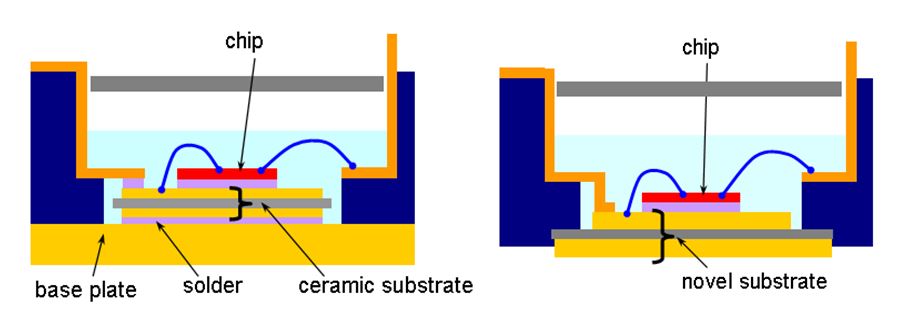
Fig. 5. The comparison between conventional structure (left) and 7th generation structure (right).
4. Conclusion
7th generation IGBT, RFC diode and novel structure were applied to the 7th generation industrial IGBT module. In IGBT chip, reduction of the static and dynamic losses without sacrificing the short-circuit capability was realized, together with the improvement of the trade-off relationship between Eon and recovery dv/dt. In diode, reduction of the static and dynamic losses without snap-off and oscillation phenomena was realized. In package, new smaller package is realized without inducing problems of surge voltage.
As a result, 7th generation IGBT module makes it possible to double the current rating with the same package size. The weight is reduced by 45% from conventional module.
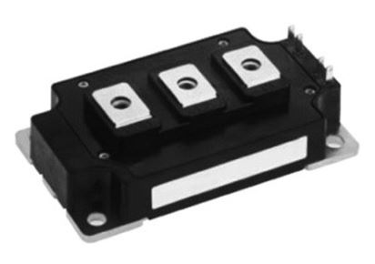
These technologies are applied to the following package, for example.
5. Reference
[1] K. Nakamura et al. “Evaluation of Oscillatory Phenomena in Reverse Operation for High Voltage Diodes”, Proc. ISPSD 2009, pp. 156-159, Barcelona, Spain
[2] F. Masuoka et al. “Great Impact of RFC Technology on Fast Recovery Diode towards 600 V for Low Loss and Hogh Dynamic Ruggedness”, Proc. ISPSD 2012, pp. 373-376,
Bruges, Belgium
[3] H. Takahashi et al. “Carrier Stored Trench-Gate Bipolar Transistor (CSTBT) –A Novel Power Device for High Voltage Application-“, Proc. ISPSD 1996, pp.349-352
[4] Y. Haraguchi et al. “600V LPT-CSTBTTM on Advanced Thin Wafer Technology”, Proc.
ISPSD 2011, pp. 69-71, San Diego, California, USA
[5] S. Honda et al. “Next Generation 600V CSTBTTM with an Advanced Fine Pattern and a Thin Wafer Process Technologies”, ISPSD 2012, pp. 149-152, Bruges, Belgium